Glossary
is a powerful technique for studying the structures of crystal samples in a wide variety of research and process chambers.
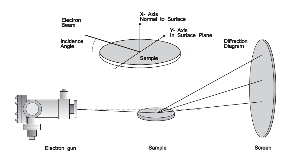
 Electrons can be diffracted by a surface in a similar way as visible light, except that the associated wavelength is much smaller. Low energy electrons have a wavelength that is in the order of atomic spacing and can be diffracted by lattice atoms. High energy electrons have a wavelength much smaller than the lattice spacing and diffraction conditions can be reached simply by setting the incident beam at a very small incidence angle to the surface. The diffracted electrons build a diagram consisting of a superposition of spots at Bragg angles for the bulk material, streaks from the surface diffraction, and Kikuchi lines from channeling effects.
 The ability to monitor variations of the diagram during deposition is most valuable. RHEED delivers real time detailed information about the crystal structure of the bulk and the smoothness and crystalline quality of the surface layer with a sub-monolayer resolution. When used in a deposition device, the diffraction diagram instantly displays the surface modifications. The intensity of diffraction spots or streaks is used to monitor the deposition at a layer-by-layer sensitivity (technique named RHEED oscillations).
RHEED is the premium choice technique for growth monitoring since multiple different parameters can be captured simultaneousley in situ, and in real time.
The video feed can be analyzed in a suitable RHEED acquisition software. Here, the area of interest can be set on the RHEED diagram to follow the signal intensity variations, which can be instantly converted into growth rate and layer thickness.
- Beam rocking capability to electronically fine adjust the incidence angle.
- A high beam energy option for operation of RHEED in large vessels, or in order to work with poorly diffracting samples (high energy allows more bulk diffraction) and samples with poor and complex crystal structures (such as textures, nanofibers). High energy guns of 100 keV are also used for gas diffraction.
- Addition of pumping stage (differential pumping) to the electron gun allows it to work under poor vacuum conditions (TorrRHEEDTM), a common requirement for many deposition systems, such as PLD, IBD, MOMBE and more.
- Blanking the electron beam (beam blanking) allows fast control of the beam (switching on/off) that can be used for rotating samples and to drastically reduce the electron impact effects on electron sensitive surfaces (organic materials).
This method refers to the measurement of specific energy losses suffered by a Primary Electron (PE) traveling through a surface or inside a solid target. All interactions belong to elementary excitation in solids that theoretically describe quantified interactions of the PE with the solid bulk and surface. Each kind of interaction has its own energy, meaning that the PE will lose a characteristic amount of energy for each excitation, which is the basic feature of EELS.
The most common interactions are:
- ionization of a core atomic level (followed by X-ray or Auger emission)
- the excitation or ionization of outer energy levels leading to intra- and inter-band transitions
- the plasmon excitations of the electron gas of the valence / conduction band. Experimentally, plasmon excitation are normally dominant.
There are two different ways to measure energy losses, and their results are very different:
- In Transmission, where the PE crosses a thin sample as found in Transmission Electron Microscopy (TEM). This technique is referred to as transmission Electron Energy Loss Spectroscopy (commonly understood as EELS).
- In Reflection, where the PE impacts a thick sample and the energy loss spectra is measured from electrons back scattered from the surface. This technique is referred to as Reflection Electron Energy Loss Spectroscopy (REELS).
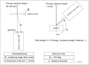
 The following figure shows two possible configurations, for transmission and for reflection. The incidence angle is normal to the surface in transmission, but it can have any orientation in reflection. An interesting geometry is using a high energy PE beam at grazing angle to the surface (RHEED geometry) and a RHEA analyzer.
Although both techniques generate similar excitations, they differ by the fact that in transmission by choosing proper sample thicknesses the background of electrons scattered inside the target is kept very low as compared to energy loss intensities. In contrast, all electrons in reflection mode must be scattered by a large angle. Therefore a larger background of scattered electrons is added to the energy loss signals. Fortunately, this background is negligible for energies near the PE energy. Thus, Characteristic Energy Losses (CEL) like plasmon and band transition can be well measured in reflection mode whereas the larger loss energies corresponding to deeper core level excitation will be superposed to a large background of scattered electrons.
The dominant CEL structures measured in reflection are Plasmons, low energy ionization levels and band transitions. The corresponding loss energies do not depend on the atomic number Z but are governed by the outer shell structure of the solid, thus making CEL very sensitive to the chemical environment of surface layers.
For REELS, energy analyzers with very good energy resolution are required. The analyzers should reach this resolution especially at higher PE energies in the keV range, and, additionally work in constant energy resolution mode (providing constant resolution at all energies). Standard CMA are therefore not well suited for this kind of operation.
In contrast, all STAIB Instrument energy analyzers are powerful REELS analyzers.
Principle
The sample is illuminated with X-ray radiation of sufficient energy to create core level ionizations of the atoms. The photon energy is transferred to the electron, with some leaving the sample as photoelectrons. The kinetic energy of the emitted photoelectron is given by the difference between photon energy and binding energy of the electron in the sample. Unlike for X-ray or Auger emission, the energy of the photoelectron depends on the X-ray energy used. As X-ray radiation is almost monochromatic, the energy of the measured line can be simply converted into binding energies.
Technique
An X-ray source producing quasi-monochromatic radiation (using Al or Mg anodes) is used to generate photoelectrons of different energies. The energy of the emitted electrons is analyzed by a highly sensitive, high energy resolution energy analyzer. The filter energy is scanned over the photoelectron lines and the signal is detected using an electron multiplier. The measured energy distribution is digitalized and displayed by a computer program. Data are saved in various formats for processing and quantification.
Set up
The minimum configuration requires an X-ray source and a high resolution energy analyzer suitable for XPS. The X-ray source is equipped with two anodes, Al and Mg, delivering different photon energies so that the photoelectron lines can be differentiated from the Auger lines (at fixed kinetic energy). Modern analyzers have selectable energy resolution and large working distance (good sample clearance). Having the electron source built into the analyzer provides ease of use and alignment, with full AES capability on a single flange. The STAIB DESA- family is optimized for XPS and AES.
Useful options
- It is important to analyze clean, contamination free samples. The most practical and universal cleaning method is the use of an ion beam (of Argon or other heavy gases) to sputter away the surface layers (which are mostly contamination). The same ion source can be used for Ion back-Scattering Spectroscopy (ISS).
- Computer control of the analyzer system allows users to pre-set series of measurements (i.e. for over night).
- When combined with a micro-focus source, full Auger capabilities become available, including AES, SEM and SAM.
- A special low energy electron source can be used for charge compensation on isolating samples.
Principle
The sample is bombarded with an electron beam of sufficient energy to create core level ionizations, leaving a hole in a specific electronic shell. Recombination occurs by filling the hole with an electron from an outer energy level. The released energy is carried outside either by an X-ray photon or another electron from the atom, the Auger electron. Like for X-ray emission, the energy of the Auger electron is characteristic of the atomic element and does not depend on the energy or kind of excitation used.
Technique
The sample (gas or solid) is bombarded by a focused electron beam of 3 to 10 keV energy. The energy of the emitted electrons is analyzed by a highly sensitive energy analyzer, in which the filter energy (so called Pass Energy) is scanned over the Auger lines and the signal is detected using an electron multiplier. The measured energy distribution is digitalized and displayed by a computer program. Data are saved in various formats for processing and quantification.
Set up
The minimal configuration is an electron gun of 3-10 keV energy and an energy analyzer. The best design is to have the electron gun built into the analyzer. Modern analyzers have a selectable energy resolution and large working distance (offering good sample clearance). The STAIB ESA-family is optimized for AES and provides the most advanced compact analyzer design on the market.
Useful options
- It is important to analyze clean, contamination free samples. The most practical and universal cleaning method is the use of an ion beam (of Argon or other heavy gases) to sputter away the surface layers (which are mostly contamination).
- Ion sources can also be used for Ion back-Scattering Spectroscopy (ISS), and AES depth profiling.
- Excitation for AES can be operated with any electron source, provided it delivers a very low noise, stable beam in the correct energy range. When combined with a micro-focus source (delivering a small spot of high spatial resolution), very small sample areas can be analyzed, down to about 100 nm. Scanning Electron Microscopy (SEM) and Scanning Auger Microscopy (SAM) utilize a beam that is scanned over the sample, to map the surface elements.
- Computer control of the analyzer system allows users to pre-set series of measurements (i.e. for over night).
- Special systems have been designed to perform AES measurements at higher vacuum pressures, i.e. see AugerProbeTM.
- Very compact AES analyzers, with small diameter and large working distance, can be used in systems where the space available is very tight (like MBE chambers).

