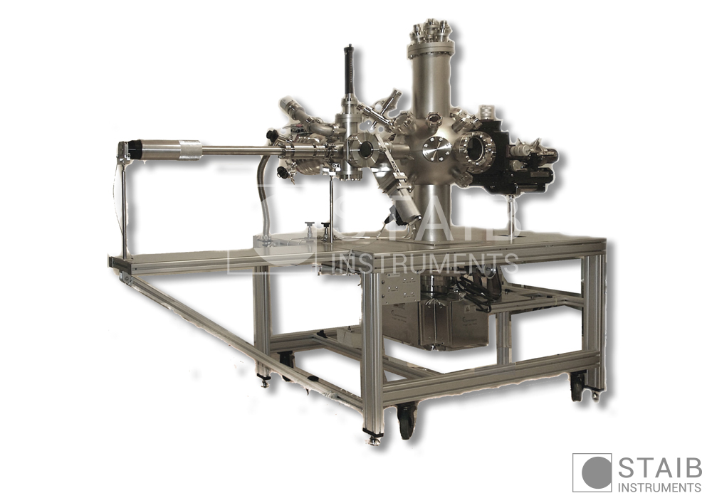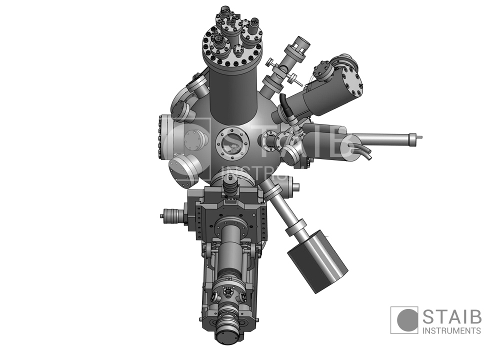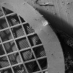
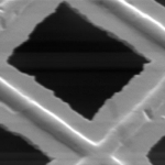
 STAIB Instruments offers a wide range of reliable, affordable Surface Analysis Packages, including systems for AUGER Electron Spectroscopy (AES), Photoelectron Spectroscopy (XPS, UPS), Scanning Electron Microscopy (SEM), Scanning AUGER Microscopy (SAM) and RHEED.
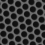
STAIB Instruments provides SEM packages to image a wide range of resolutions (spot sizes 200 nm to 5 μm) and energies. The packages are designed to add to existing UHV chambers or to use as a lab stand-alone application chamber. Each package includes a STAIB Micro- or Nanofocus electron source, fully UHV compatible and reliable over years of use, coupled with a secondary electron detector and integrated with state-of-the-art, easy-to-use software for instrument control and sample imaging. Any Micro- or Nanofocus SEM package can be combined with a STAIB energy analyzer for complimentary Scanning Auger Microscopy (SAM).
The STAIB SEM package consists of:
- Electron source with
- full octopole stigmator / deflection stage and double alignment
- High voltage and beam control supply
- Scanning electronics
- Secondary Electron Detector – scintillation type with low noise pre-amp
- Software for integrated instrument control and sample imaging
- USB gun control and USB2 scanning / acquisition interface
- Windows™ PC with 22” TFT display
- The system can be interfaced with all STAIB Auger Analyzers (see SAM package).
Software for integrated control and sample imaging
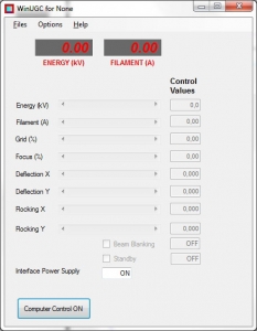
- The Windows™ based software provides complete control of the main source parameters. All parameter sets can be saved and retrieved through USB interfaces.
- The operator can choose among several preset configurations for energy and beam current.
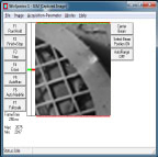
- Acquired images can be saved, up to 5 frames per second, and exported.
- Images can be calibrated for magnification (optional).
STAIB Instruments provides Scanning Auger Microscopy (SAM) packages. The packages are designed to add to existing UHV chambers or to use as a lab stand-alone application chamber. Each package includes a STAIB Micro- or Nanofocus electron source, fully UHV compatible and reliable over years of use, coupled with a STAIB Auger analyzer, easy-to-use software for instrument control and sample imaging.
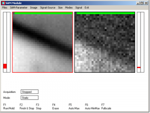
The STAIB SAM package consists of:
- Electron source with
- full octopole stigmator / deflection stage and double alignment
- High voltage and beam control supply
- Scanning electronics
- STAIB AUGER analyzer
- DESA 100/150 or ESA100
- Alternatively electron source and analyzer in one unit:
- ESA150M the unique STAIB Auger Microprobe Analyzer
Combining a high sensitivity AUGER analyzer with a coaxially mounted Microfocus.
- ESA150M the unique STAIB Auger Microprobe Analyzer
- Software for integrated instrument control, sample analysis and sample imaging
- USB gun control and USB2 scanning / acquisition interface
- Windows™ PC with 24” TFT display (optional)
- The system can be interfaced with a STAIB Secondary Electron Detector – scintillation type with low noise pre-amp to form a complete SEM / SAM unit.
- The Windows™ based software provides complete control of the main source parameters. All parameter sets can be saved and retrieved through USB interfaces.
- The operator can choose among several preset configurations for energy and beam current.
- Auger map
- Auger line scan
- Auger zone scan
AugerProbeTM for in situ Real Time Elemental Monitoring and REELS Studies
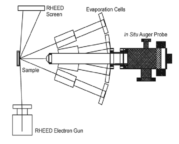
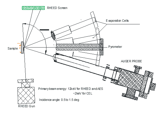
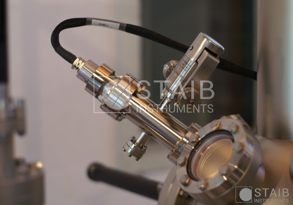
The STAIB Instruments AugerProbeTM is a uniquely designed in situ, real time monitoring tool. Designed to operate in difficult environmental conditions, like high pressure, material deposition, and long working distance (~2”), the analyzer is ideally suited for monitoring in growth chambers. An electron source is needed for Auger excitation. A glancing angle STAIB RHEED electron source can be used for excitation to provide in situ, real time, coincident RHEED structural data and Auger elemental composition information, both observed during the growth process. Substrate processing can be monitored. Process parameters can be tuned. Material behavior can be studied, with simultaneous RHEED diffraction and Auger analysis during deposition. Individual element composition can be observed during the growth process and can be further quantified (calibrated and physical) using a new modeling taking into account the different matrix effects. With an appropriate excitation source, REELS spectra can also be obtained from the growing material.

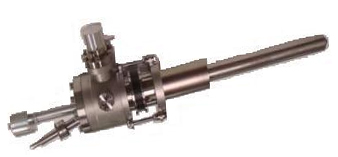
Probe Advantages include:
- Designed to fit process chambers without interference.
- Excellent & adjustable energy resolution to optimize Auger line signals and detailed REELS.
- Fast acquisition for real time elemental Growth Profile.
- Large working distance & small diameter.
- Rugged construction to operate during growth from UHV up to several mTorr.
- Stable and reproducible operation over long periods of time as required for MBE applications.
- Mounts on most sample facing, CF ports.
- A normal or near normal port on a growth chamber – see below.
- Mounted on a load lock chamber or a transfer line port for pre- and post-growth sample evaluations.
- CF-63 (ID) / 4.5″ (OD) flange standard, others available.
Optionally, the AugerProbeTM can be located on a load lock chamber or a transfer line port for pre- and post-growth sample evaluations.
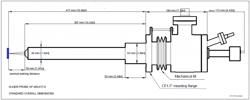 Requires STAIB electron source for Auger excitation for best stability and signal-to-noise figures.
- Glancing angle (RHEED gun) or non-glancing gun (2-10 keV).
- Low energy capability for possible REELS use.
References:
- Staib, In situ Real Time Auger Analyses During Oxides and Alloy Growth Using a New Spectrometer Design, JVSTB, May/June 2011, 29(3), doi:10.1116/1.3562195.
- Calley, et al, In situ Auger probe enabling epitaxy composition control of alloys by elemental surface analysis, JVSTB, May/June 2013, dx.doi.org/10.1116/1.4798653.
- P. Staib, In Situ Energy Loss Spectroscopy, A Novel Approach to the Characterization of Surfaces during MBE Growth, AVS Meeting 2014, Abstract # 5399.
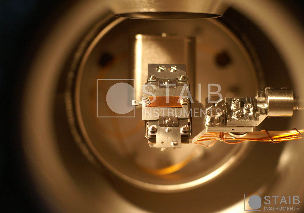
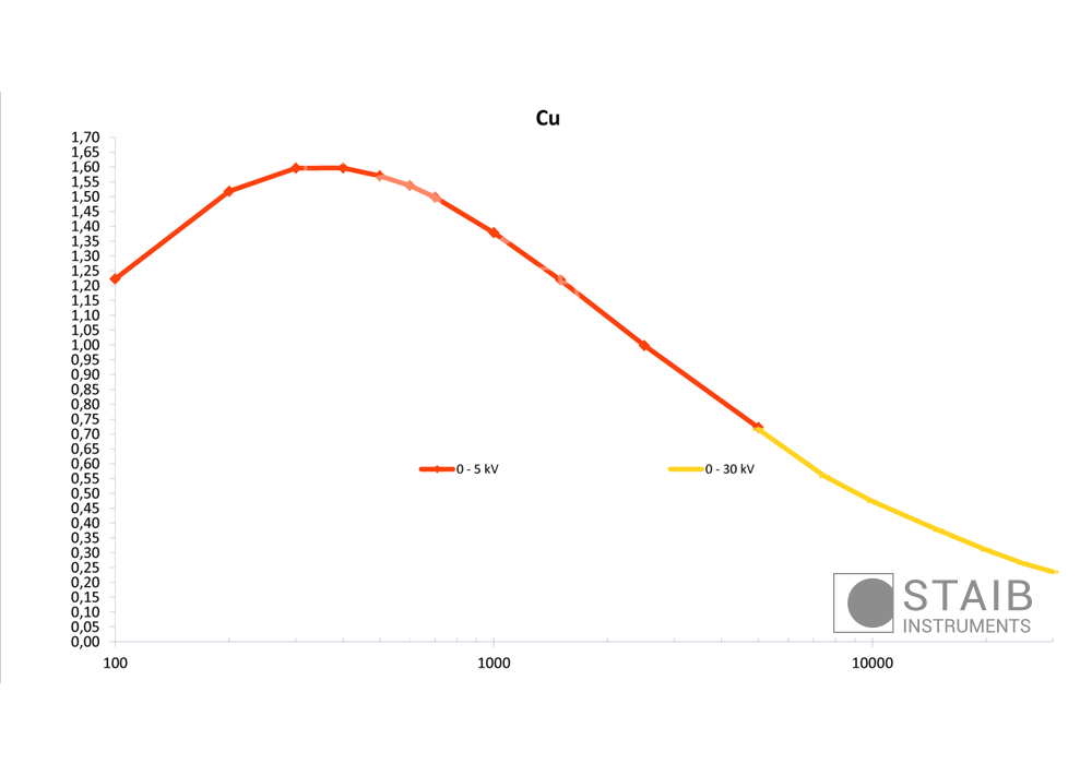
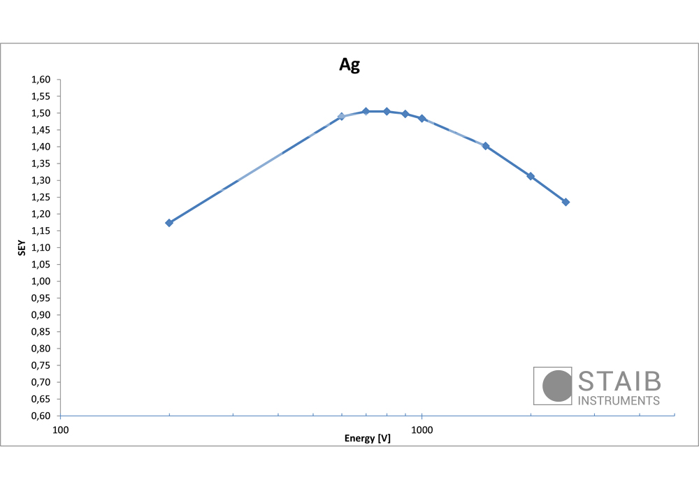
STAIB Instruments has developed a new analyzer for quantitative measurement of Secondary-Electron Yield (SEY), Secondary Electron Distribution (SED), and Backscattered Electron Yield
The STAIB SEY-Analyzer package consists of the following components:
- SEY-Analyzer with 180° multi-grid for quantitative measurement of secondary electron yield and distribution
- Integrated Sources
- Integrated primary electron source for continuous or pulsed mode operation
- Integrated low energy electron source for charge compensation
- Integrated ion source for cleaning and charge compensation
- Control and aquisition Capability
- Gun control and analysis modules
- Control and data acquisition software
Integration of the SEY-Analyzer into a multi chamber STAIB MultiTechTM System provides the user with the following techniques:
- SEY-Analyzer
- Secondary Electron Yield analysis
- Secondary Electron Spectroscopy
- STAIB MultiTechTM System Plus based on DESA 150
- Scanning Auger (SAM)
- XPS, UPS
- UHV Secondary Electron Microscopy (SEM)
- EELS
- PEEM

